
Contact Probes
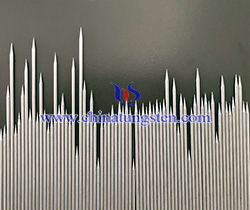
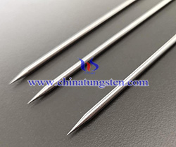
Both LED chip probing and map/sorting technology are significant during LED product manufacturing process. The contact probes are mainly utilized in chip probing for characterizing LED opto-electronic output characteristics such as output power, emission wavelength, voltage, ESD and etc., then to do sorting into variant bins for further assembly process. They are important in back end process for LED chip quality control and cost reduction.
Applications
1.Suitable in the probe testing LED chips for obtaining opto-electronic output characteristics;
2.Suitable in the probe testing VCSEL, EELD, DFB chips for obtaining opto-electronic output characteristics.
3.Suitable in the probe testing photo-sensitive devices such as Photodiode (PD), Phototransistor (PTR), Schottky diode and Zener diode for obtaining opto-electronic output characteristics.
Main Materials
1.PA alloy
2.PT alloy
3.GC alloy
4.BeCu alloy
5.Tungsten carbide alloy
6.Pure tungsten
7.Tungsten rhenium alloy
8.Plastic
If there is any interest in tungsten products, please feel free to contact us through the following methods.
Email: sales@chinatungsten.com
Tel.: +86 592 512 9696/+86 592 512 9595
More info>>