
CTIA Tungsten Needle in Scanning Probe Microscopy and Nanocharacterization
CTIA tungsten needle serves as a core functional component in scanning probe microscopy and nanocharacterization, enabling atomic-scale imaging, mechanical/electrical testing, and localized structural analysis. In systems such as Scanning Tunneling Microscopy (STM), Atomic Force Microscopy (AFM), Field Ion Microscopy (FIM), Scanning Near-field Optical Microscopy (SNOM), and nanoprobing platforms, the tip material directly determines resolution limits, signal stability, and long-term reliability.
With a high melting point (~3410 ℃), high elastic modulus (~400 GPa), low vapor pressure, and stable electronic structure, CTIA tungsten needle maintains tip geometry consistency, uniform work function, minimal thermal drift, and strong resistance to atomic migration at the nanoscale, providing a solid material foundation for high-precision imaging and characterization.
In these applications, extremely tight control is required over tip curvature radius, surface defect density, grain uniformity, and electrical consistency. Tip radius is typically maintained within 20–50 nm, while atomic-resolution imaging requires sub-nanometer precision, with surface roughness (Ra) ≤2–5 nm.
Through high-purity material selection, grain refinement, nanoscale electrochemical etching, and precision tip fabrication, CTIA ensures controllable tip coaxiality, curvature radius, and crystallographic structure. This enables stable electron/ion tunneling currents, consistent mechanical feedback signals, and reliable field emission performance over extended operation, supporting both research and industrial nanocharacterization with high precision and repeatability.
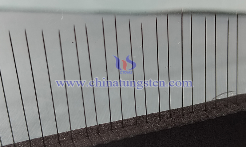
In Scanning Tunneling Microscopy (STM), tungsten needle enables atomic-scale imaging through quantum tunneling. When the tip–sample distance is below 1 nm, a tunneling current is generated. Smaller tip radius and stable electrical properties reduce current fluctuations and improve imaging resolution. In advanced applications, tip curvature is typically controlled below 20 nm to achieve atomic resolution.
With a melting point of 3410 ℃, elastic modulus of ~400 GPa, work function of ~4.5 eV, and vapor pressure below 10?? Pa at 2500 K, tungsten exhibits superior thermal stability, mechanical strength, and low surface diffusion under Ultra High Vacuum (UHV) conditions. It resists thermal migration, recrystallization, and tip blunting even under high current density. Through electrochemical etching and field evaporation, nanoscale tips with atomically clean surfaces can be obtained. High purity and uniform grain structure further reduce surface defects, improving current stability and experimental repeatability.
2. Tungsten Needle for AFM (Atomic Force Microscopy)In Atomic Force Microscopy (AFM), tungsten needle measures surface morphology and mechanical properties through short-range tip–sample interactions. In contact or tapping modes, the probe must withstand continuous mechanical loading while maintaining geometric stability. In Conductive Atomic Force Microscopy (C-AFM), the tip also carries nanoampere-level current, requiring both mechanical strength and electrical consistency.
With Vickers hardness of ~350–500 HV and elastic modulus of ~400 GPa, tungsten needle provides high stiffness, reducing plastic deformation and lateral drift during scanning. Its stable resistivity (~5.6×10?? Ω·m) enables reliable current transmission without coatings, avoiding contact resistance variation caused by coating wear. In nanoindentation and friction testing of hard materials, tungsten needle can withstand over 10? contact cycles while maintaining tip integrity, demonstrating excellent fatigue resistance and dimensional stability.
3. Tungsten Needle for FIM (Field Ion Microscopy)In Field Ion Microscopy (FIM), tungsten needle operates under high voltage to generate local electric fields of ~10? V/m, enabling gas atom ionization imaging. Tip curvature directly affects the field enhancement factor, requiring nanoscale tip fabrication and atomic-level structural stability under extreme fields.
Tungsten’s low surface diffusion coefficient and high melting point suppress atomic migration and tip evolution under high-field conditions. Single-crystal tungsten tips can achieve atomic resolution at low temperatures, with the (110) orientation offering more stable atomic layer evaporation and reduced emission noise. High-purity tungsten further minimizes current fluctuations, improving imaging repeatability and long-term stability. CTIA ensures controllable tip curvature and crystallographic orientation through nanoscale electrochemical shaping and grain optimization.
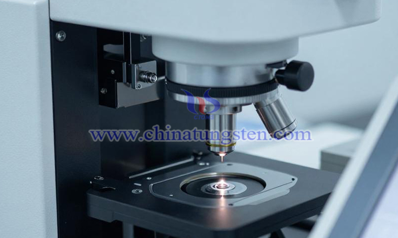
In Scanning Near-field Optical Microscopy (SNOM), tungsten needle is used for near-field optical coupling and surface scanning, requiring tip dimensions controlled at the tens-of-nanometers scale, along with smooth surfaces and geometric stability to ensure optical signal strength and spatial resolution.
With high mechanical strength (~400 GPa) and thermal stability, tungsten needle resists localized thermal stress induced by laser or optical excitation. Its low vapor pressure prevents material loss and tip degradation. Through precision polishing and grain uniformity control, CTIA achieves nanoscale smoothness, enabling stable optical coupling and repeatable scanning performance.
5. Tungsten Needle for Nanoprobing TestingIn nanoprobing applications, tungsten needle functions as a probe for localized electrical, mechanical, and magnetic measurements, requiring ultra-small tip size, stable conductivity, and high stiffness. Tip radius is typically controlled within 20–50 nm to ensure measurement accuracy and repeatability at the nanoscale.
With high thermal stability, hardness, and low vapor pressure, tungsten needle resists wear and plastic deformation during repeated micro/nano-scale scanning. CTIA ensures controlled tip dimensions, uniform conductivity, and surface defect rates below 0.5% through high-purity materials, grain refinement, and precision tip processing, providing a stable and reliable platform for nanoscale testing.
6. Tungsten Needle for Surface Electrical TestingIn surface electrical testing, tungsten needle is used for localized current measurement and potential scanning, requiring consistent conductivity, geometry, and mechanical performance. Its high hardness, low resistivity, and thermal stability ensure stable signals and tip integrity under repeated scanning and high current density conditions.
Through nanoscale polishing and heat treatment, CTIA minimizes surface defects and ensures uniform conductivity, enabling accurate nanoscale current measurements. CTIA tungsten needle demonstrates excellent repeatability, durability, and long-term stability in microelectronic characterization, localized conductivity analysis, and nanoelectronic device testing.
Across STM, AFM, FIM, SNOM, nanoprobing, and surface electrical testing applications, tungsten needle delivers high precision, repeatability, and long-term reliability through its thermal stability, mechanical strength, low vapor pressure, controllable tip curvature, and low defect surface. Leveraging high-purity materials, grain refinement, nanoscale tip fabrication, and surface optimization, CTIA provides high-performance tungsten needle solutions for advanced scientific research, industrial applications, and precision nanocharacterization.
For any inquiry, please contact?tungsten needle manufacturer: CTIA GROUP
Email: sales@chinatungsten.com
Tel: 0086 592 5129696 / 0086 592 5129595
Website: www.baixiaosheng123.com
WeChat:

More info>>